SETUP
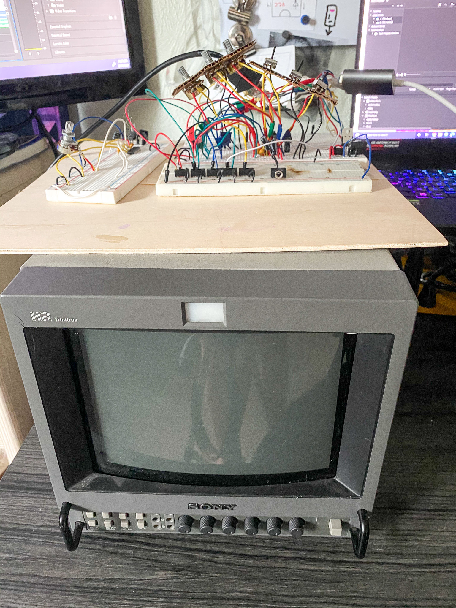
To begin working on the project, I first needed to determine my set up. I have a little Sony Trinitron CRT TV that I will be using for the visual "synthesis". It's actually professional quality thanks to my uncle who works for a news company, so it has its own potentiometer controls on the front for brightness, chroma, phase, aperture, etc. which are fun to play with on their own.
I'm using VGA video for this project, because the red, green, and blue video signals are sent independently and can therefore by manipulated. I can also manipulate the horizontal and vertical sync signals. The TV doesn't have a VGA connection, so I'm just using a converter I bought to convert VGA to s-video to send to the CRT.
To start, I drew a signal map to demonstrate what my performance setup would look like. I also drew a basic design of what the interface might look like.
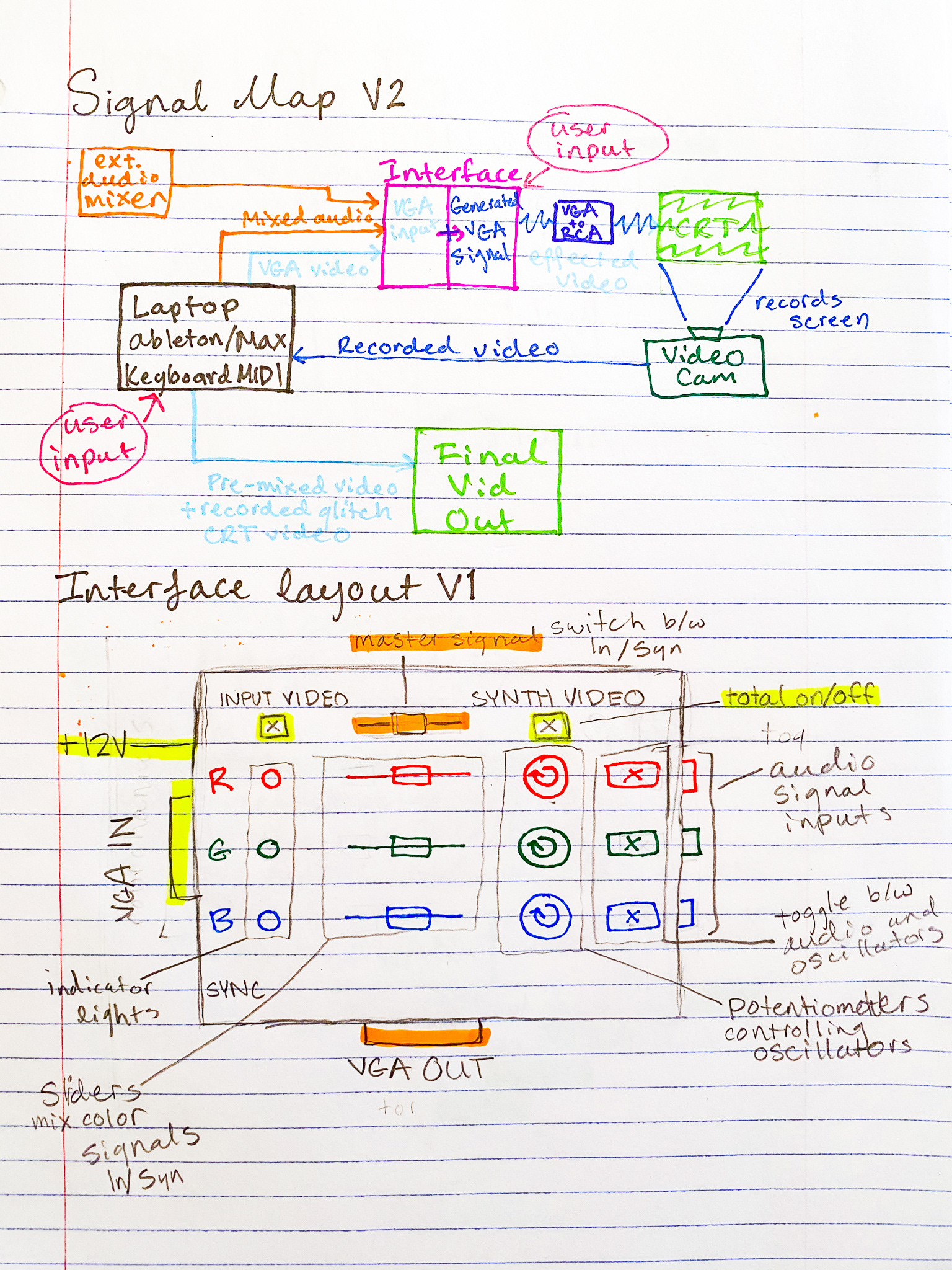
Pictured above: Signal flow map and an early interface design
My early experiments just involved interrupting a video signal (such a red) with a potentiometer. This was successful in changing the level of the video (turning on/off the red signal) but it wasn't that interesting, and the really the effect I wanted.
Pictured left: An early connector I created with a 10k Ohm Potentiometer interrupting the red video signal.

My experimentation went from blindly wiring potentiometers to having some real direction when I found the CHA/V project by Jonas Bers. Absolutely phenomenal and hilarious article. I followed his instructions and got a VGA test signal generator, a 40106 chip and some capacitors to begin experimenting. Once I really got it working it became addicting. He's not kidding about "the sickness", this is really fun to experiment with.
The VGA test signal generator acts as a video engine, creating a VGA signal that can be manipulated. The 40106 chip is actually a series of inverters that are wired in such a way that they create a pulse wave, which can be varied in frequency by a potentiometer.
I went through a lot of variations in early circuits, and made a lot of mistakes, aka burning a lot of chips. Basically, I was running 12V through the 40106 which is not something you should do because it will cause them to smoke and melt. Lesson learned, I got a voltage regulator to keep it at a nice 5V.
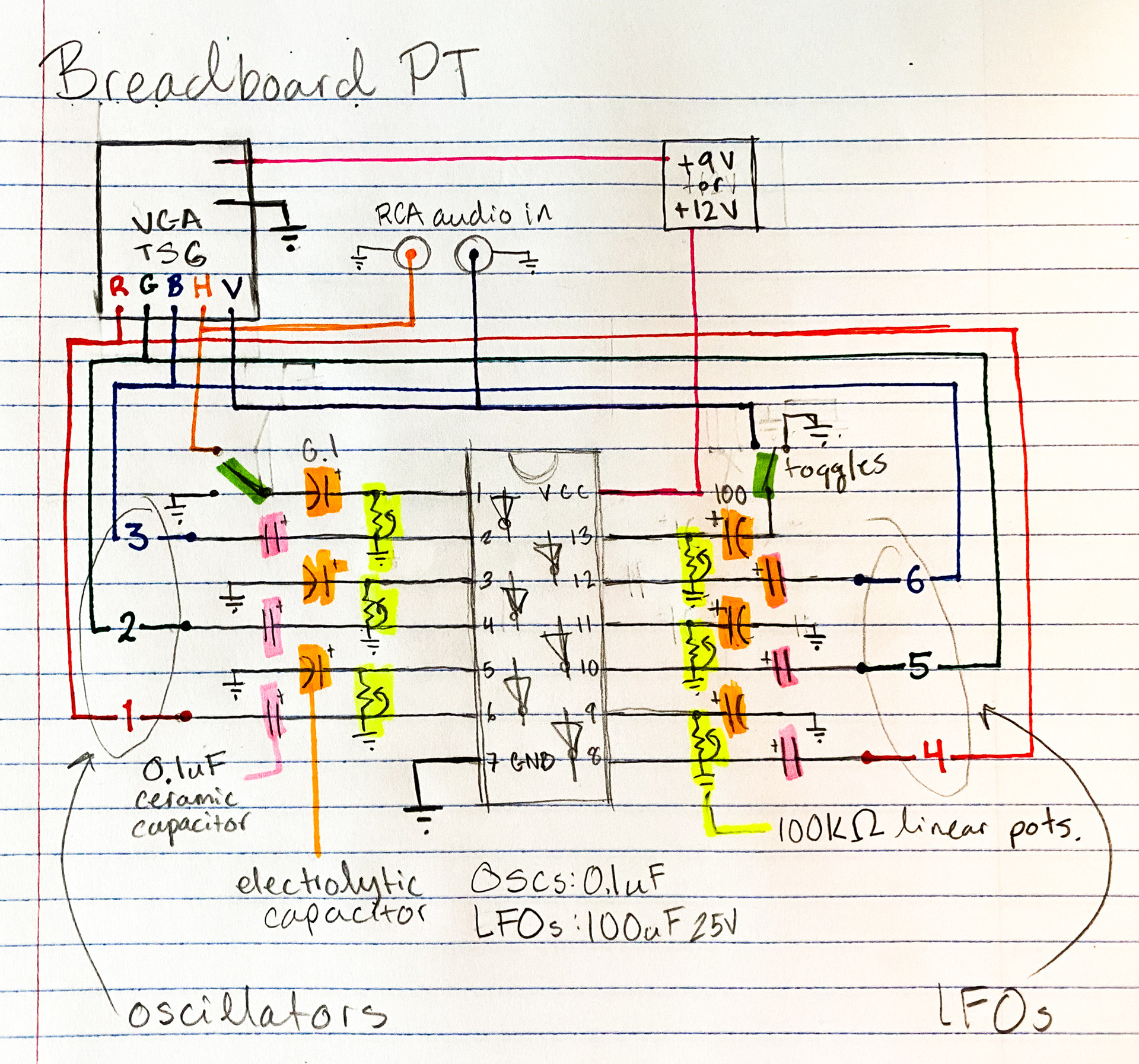
Pictured: One of my early breadboard prototype schematics. Note that this is WRONG, the VCC for the 40106 should not be anything over 5V.
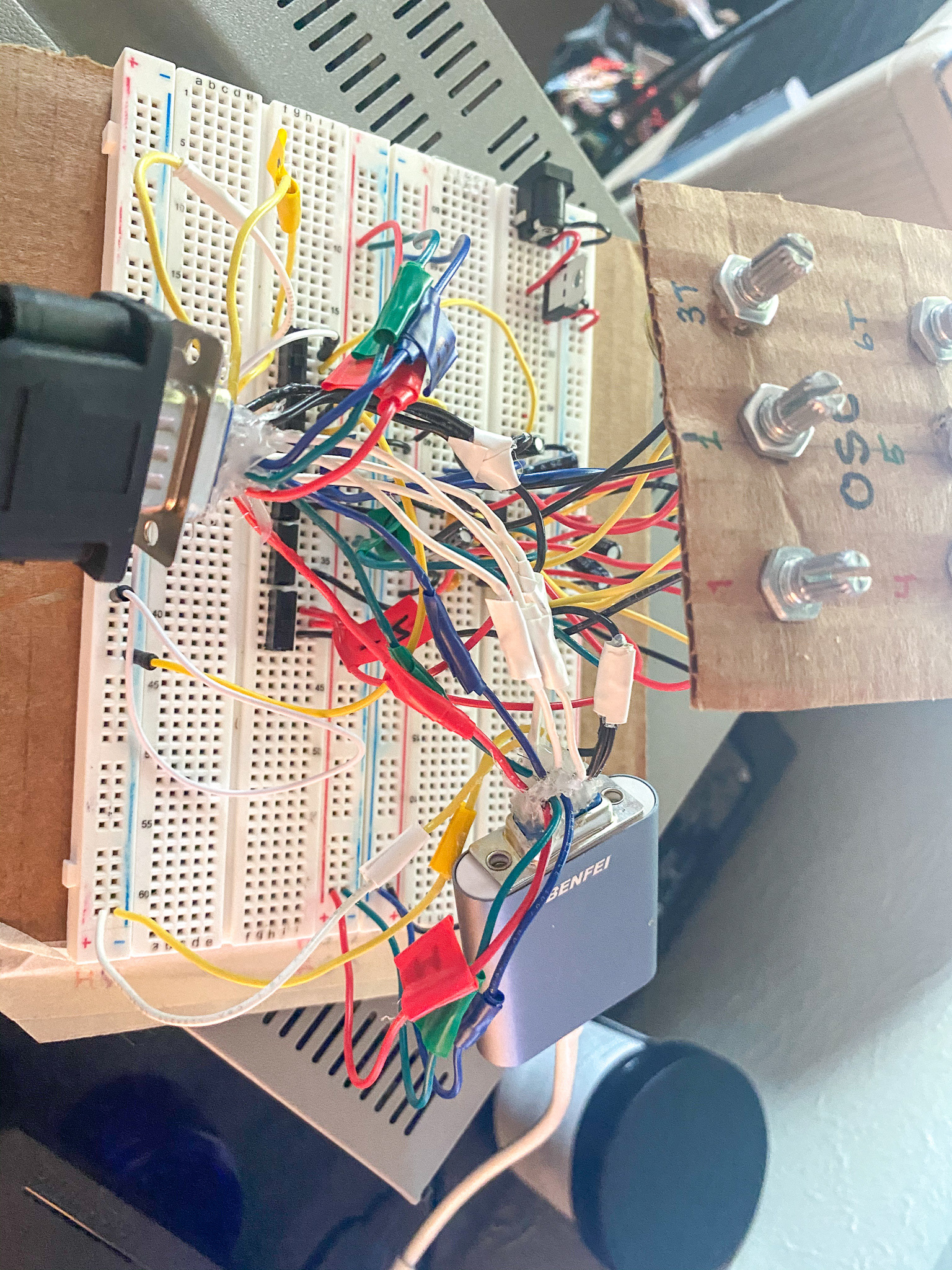
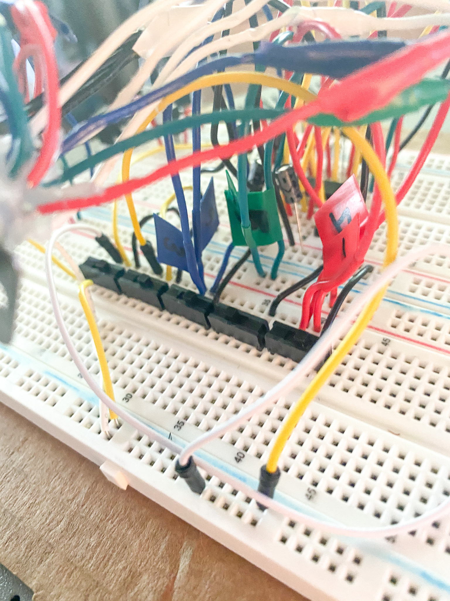
Eventually, I realized that the VGA test signal generator was just kind of getting in my way. I really wanted to manipulate my own videos from my computer. My circuit went back to a design that resembled more of my earlier prototype (the VGA in/out connector with a potentiometer interruption). This time, instead of just potentiometers varying the signals, I would be using the potentiometers to control oscillators that would manipulate the signal. This is essentially the same design as the CHA/V, but with no VGA test signal generator.
PROTOTYPING

Above: My first real breadboard prototype, shown with the TV and connections.
Below: A revised breadboard prototype and setup.
Here's a video I made using the circuit pictured above.
Live edit of Flume's Hi This is Flume mixtape visualizer. Live glitching is done with a 40106 oscillator and circuit designed and built by me. CRT TV recorded and edited by me. Minor post-processing in Premiere pro.
All music credits to Flume and original video credits to Jonathan Zawada.
All music credits to Flume and original video credits to Jonathan Zawada.
My first draft of the schematic including 6 oscillators and audio inputs, as well as patches, is below.
I am using 3.5 mm stereo jacks (wired to be mono) as my patching inputs and outputs. This way, they will be compatible with most other synthesizer and music technology. There will be 2 patch inputs for each aspect of the video (Red, green, blue, horizontal sync [vertical sync will only have one]). There will be 2 patch outputs for the extra oscillators. There will also be an external audio input that will be split into a sets of 2 patch outputs, each with their own potentiometer to control level.
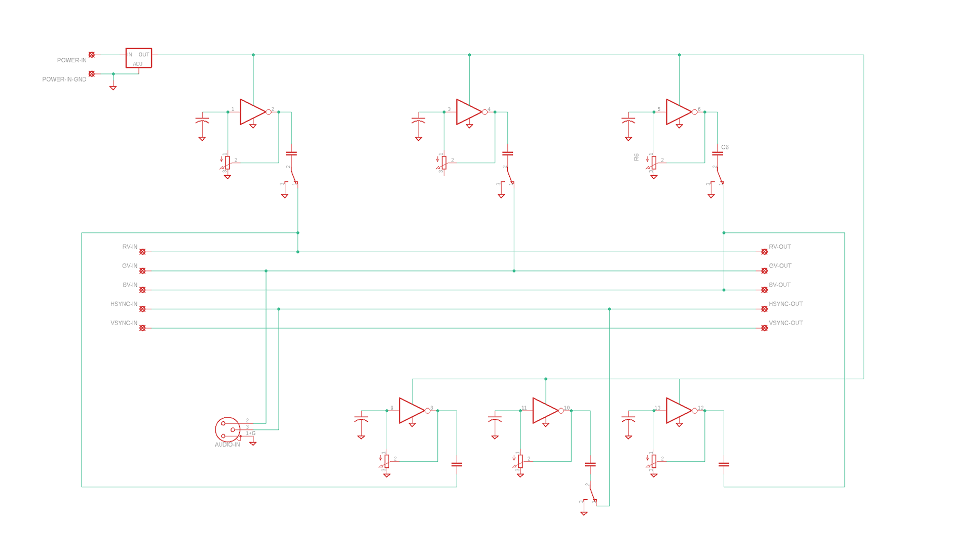
First schematic draft
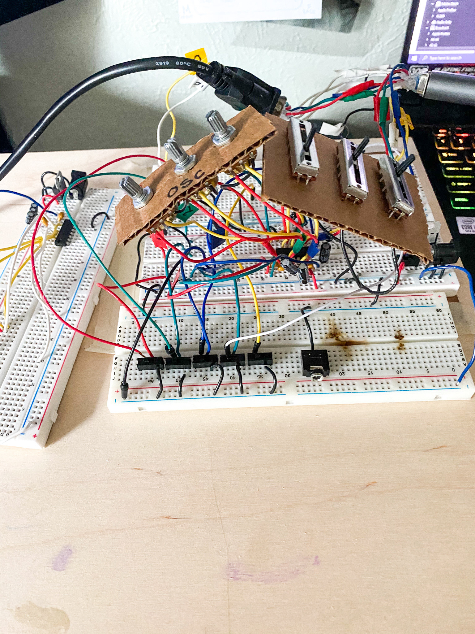
Once I ordered and received the parts I would be using in the final version, I was able to build my final cardboard and breadboard prototype.
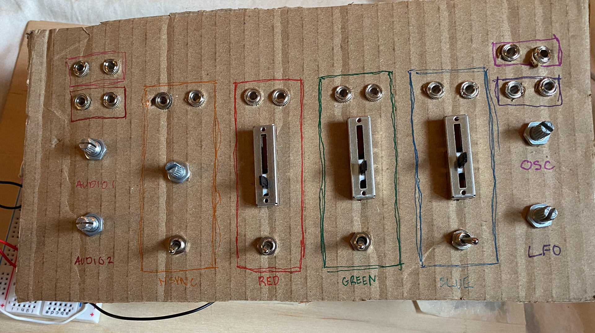
Cardboard interface prototype
Once I had the prototyping circuit ready, I moved onto designing the circuit board that I would get printed (PCB).
For my first PCB draft, I designed it with through hole solder pads in mind. I was planning to solder wires to connect the parts to the board so they would mount onto a panel interface, not directly on the board. I laid the PCB out with the IC in the center and the capacitors surrounding, and then the potentiometers and switches around it.
This design was ok, the way I laid out the parts overall was done well, but the silkscreen footprints of parts I used made it look very messy.
This design was ok, the way I laid out the parts overall was done well, but the silkscreen footprints of parts I used made it look very messy.
PCB Schematic draft
PCB Layout draft
To improve and finalize my design, I got help from electronics genius Mary West. She helped me rethink my overall design from individual solder pads (which would be messy and hard to lay flat) into a sleek ribbon cable design. She also helped me fix other things I would have otherwise not even known or thought about and perfect the final design. She also helped me format my final schematic into a professional style document.
This was my first time designing and ordering a PCB, and it's not something I was able to learn anywhere at CU. It's an overall complicated and daunting process. I cannot thank Mary enough for giving me her time and expertise to help with this process.
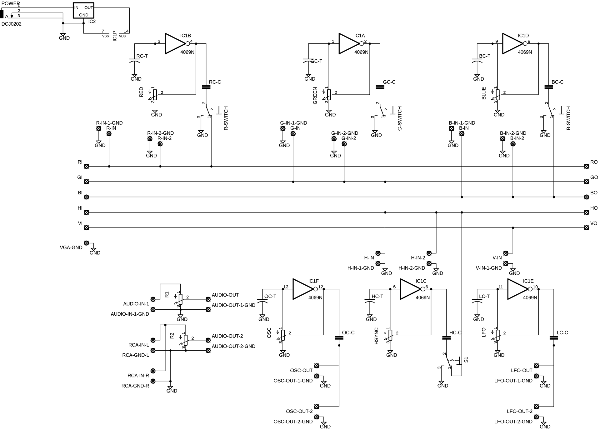
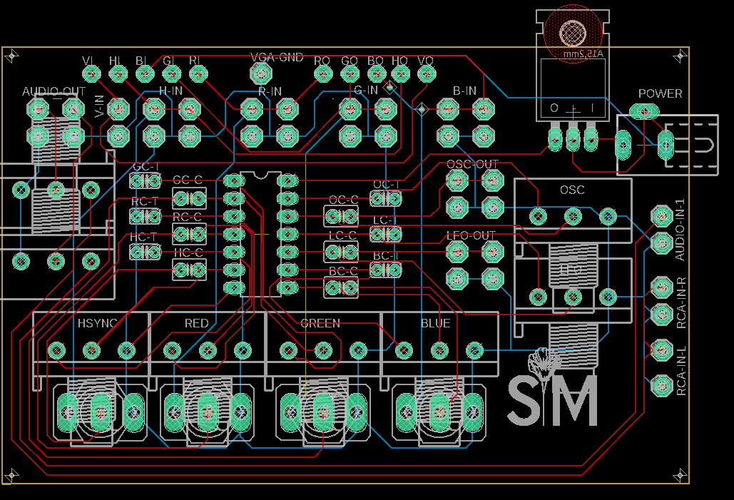
The final schematic and PCB design are below.

Final PCB Schematic
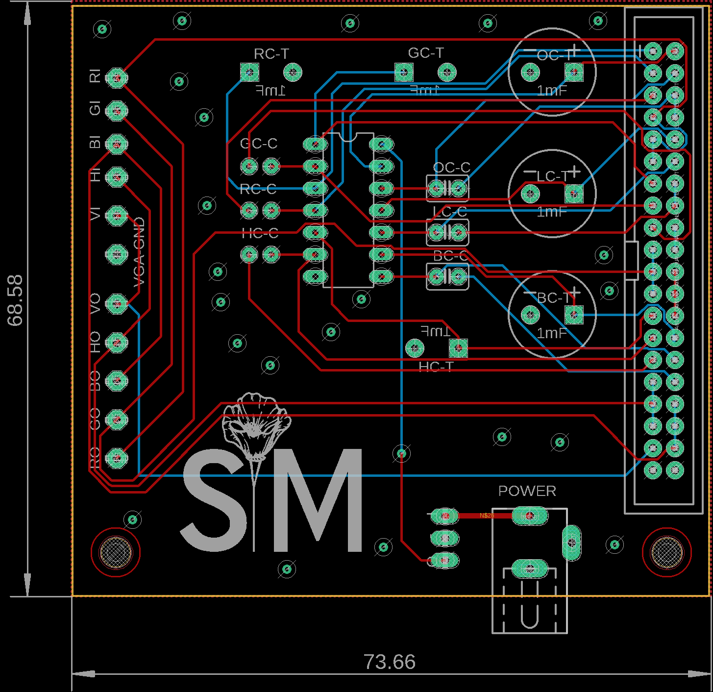
Final PCB Layout (bottom layer silkscreen is hidden for easier visibility)
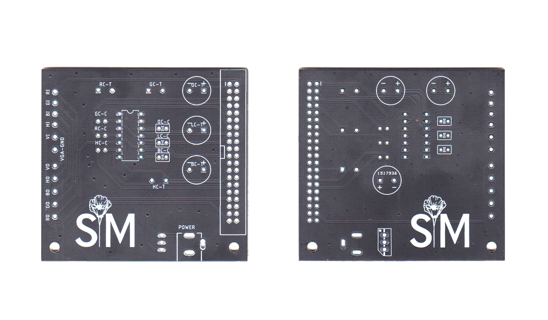
final printed boards (unsoldered) from ALLPCB
ASSEMBLY
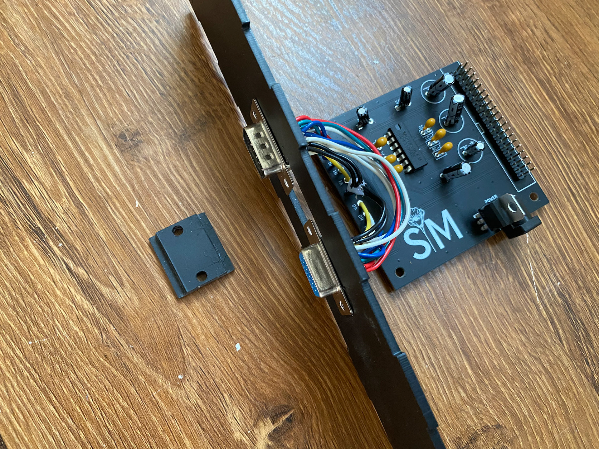
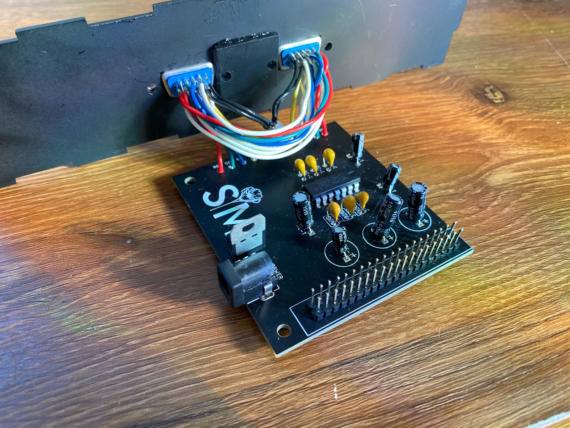
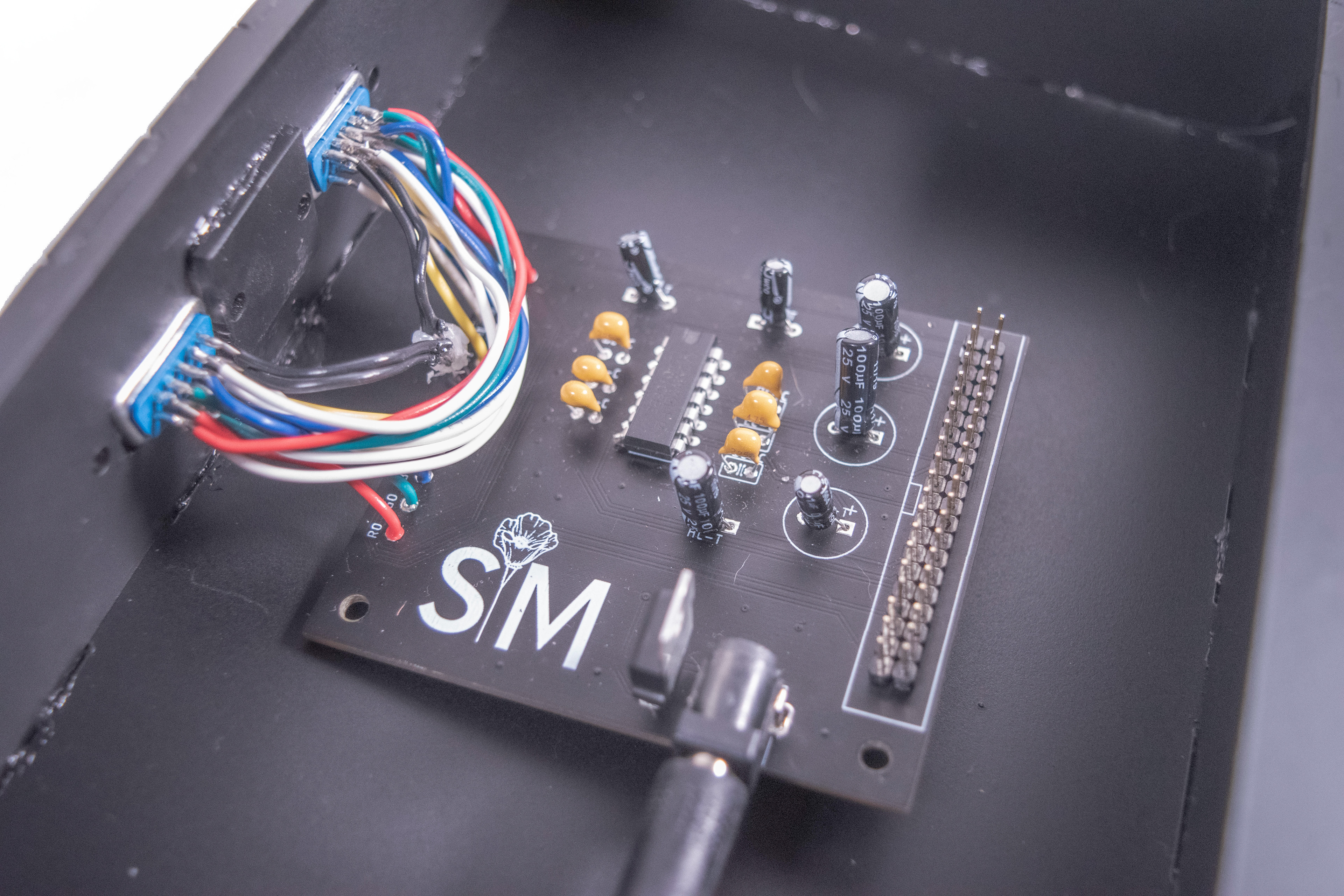
Once I received my PCBs, I could start assembling the final interface. I soldered all of my surface mount components to the PCB, which took a few tries.
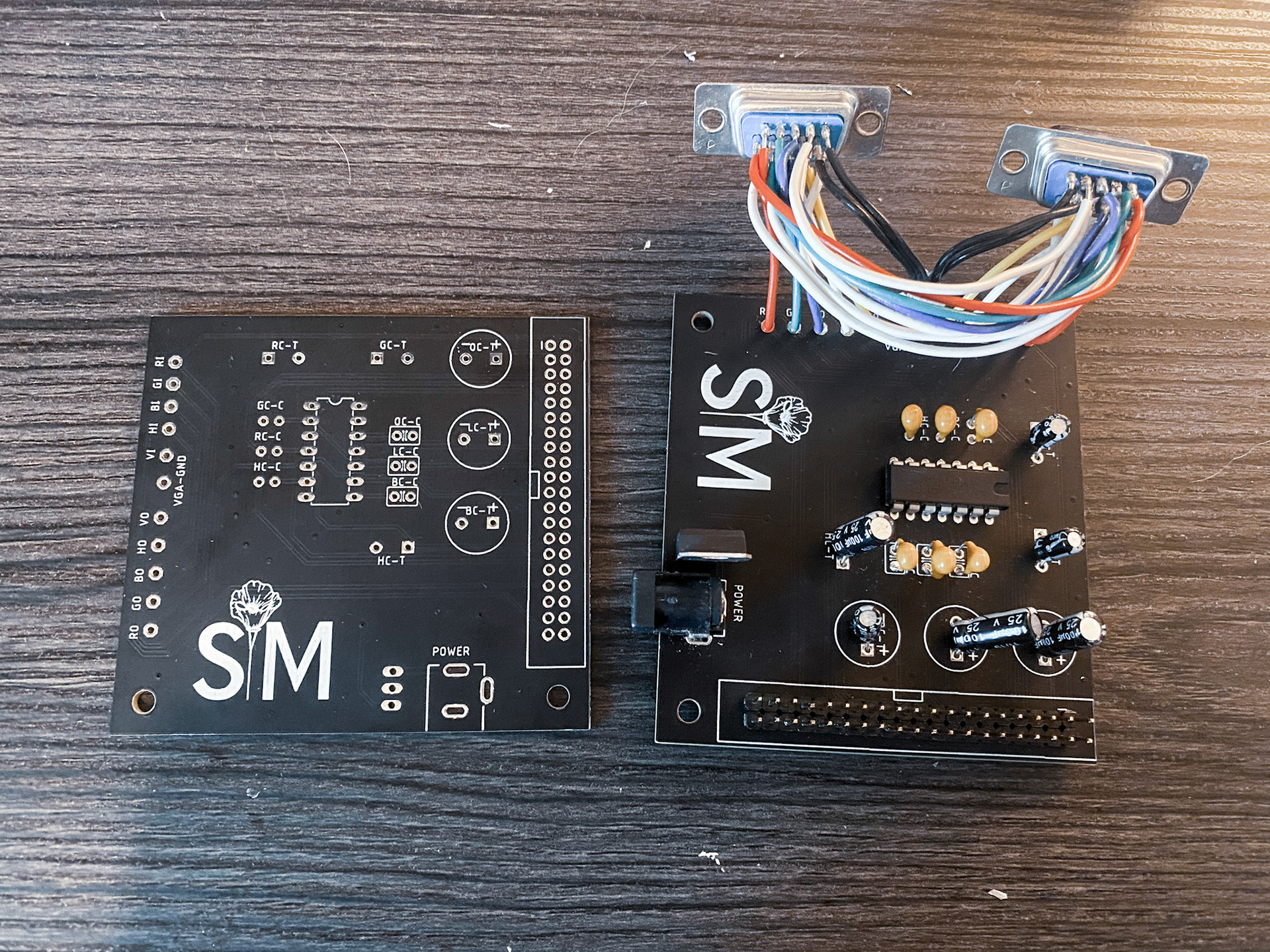
Raw PCB and fully finished PCB with mounted parts
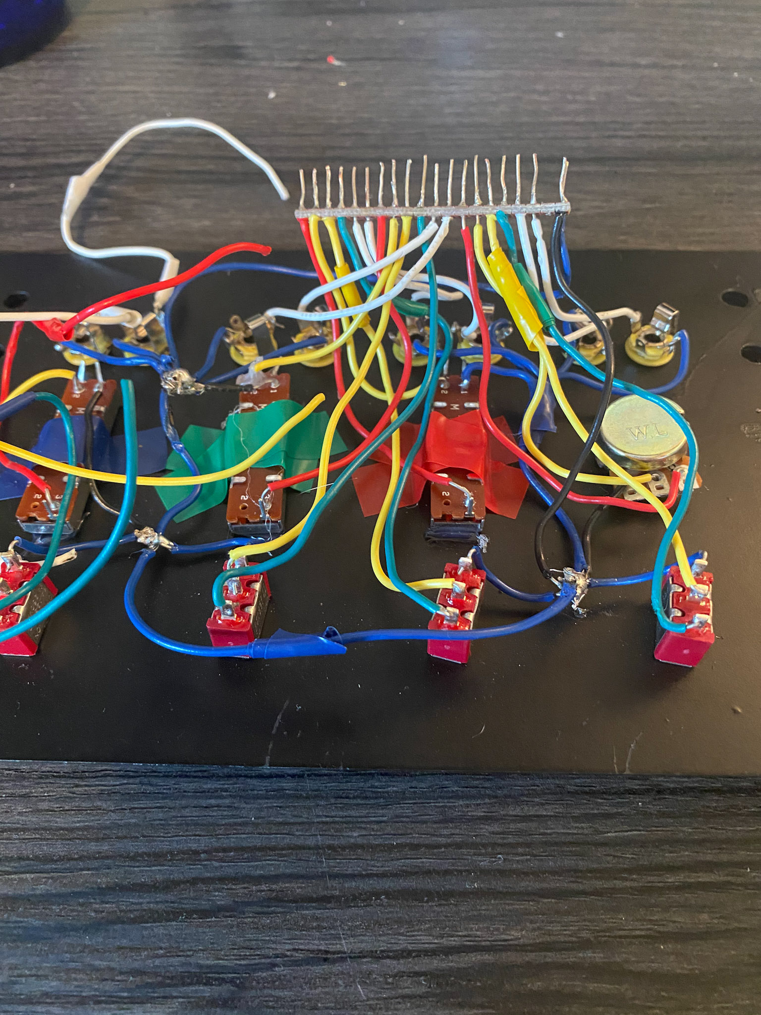
For the panel, I started by removing all my components and then spent time laying out the ground and signal wires so they would be nicely organized and lay flat. This was extremely time-consuming.
As I was assembling the first panel and testing out different features with the PCB, I noticed that my external oscillator and LFO weren't working in the way I had intended them to with my prototype. After a bit of trial, I ultimately decided to just not include them on the panel of the final interface.
Because the PCB is already printed and assembled with them, they will still exist on the board, but just won't be a feature on the interface. They were intended to be an extra oscillator that the user could patch to the colors or sync signals, but they just aren't performing well enough for me to want to keep them as part of my project. Instead, I can just use external synthesizers to patch to those signals, which provide a much cleaner signal. I figure that most users of this device would want to just plug in their own instruments anyways. Plus, this will make my interface much more straightforward and hopefully easier to use.
Because the PCB is already printed and assembled with them, they will still exist on the board, but just won't be a feature on the interface. They were intended to be an extra oscillator that the user could patch to the colors or sync signals, but they just aren't performing well enough for me to want to keep them as part of my project. Instead, I can just use external synthesizers to patch to those signals, which provide a much cleaner signal. I figure that most users of this device would want to just plug in their own instruments anyways. Plus, this will make my interface much more straightforward and hopefully easier to use.
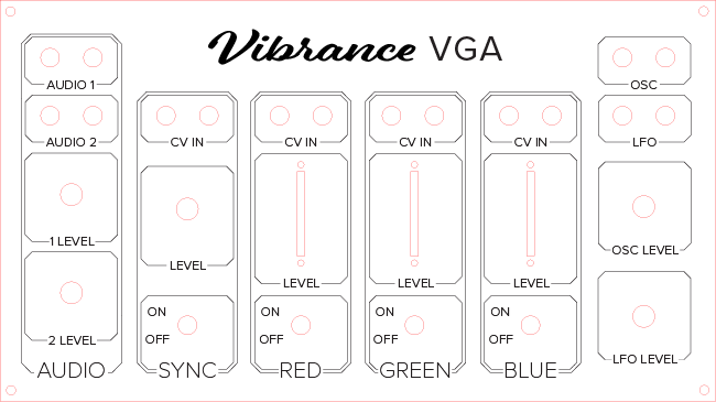
First Interface Panel Design
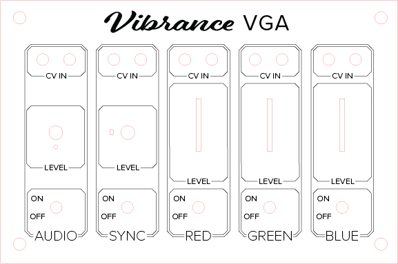
Revised Interface Panel Design
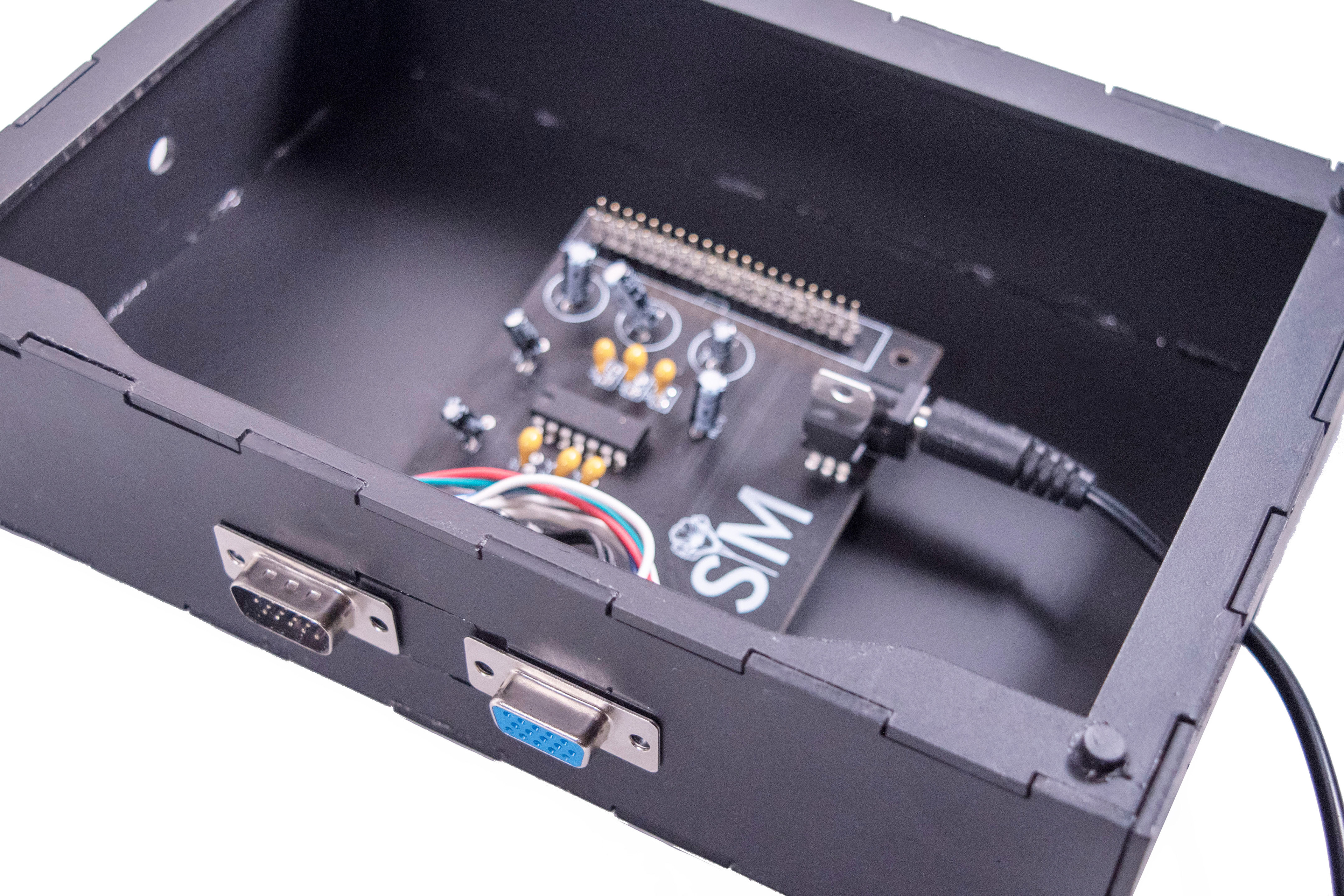
l also created an enclosure to hold my PCB and electronics. I used MakerCase to get the original box plans, then added some cutouts for connectors to audio, power, and VGA.
My design for the box is to have a top piece connected to the box that is essentially just a frame to hold the box together, and then a support for the top panel piece. This way, I can easily remove the top panel to inspect the electronics if needed.

Laser cut plans for my enclosure.
I cut the panel and enclosure designs on thin acrylic and spray painted the box components with black on both sides. I only painted the interior side of the top panel with black so the etch would be visible. I glued all of the bottom pieces together with E6000 and then spray painted again to hide glue marks.
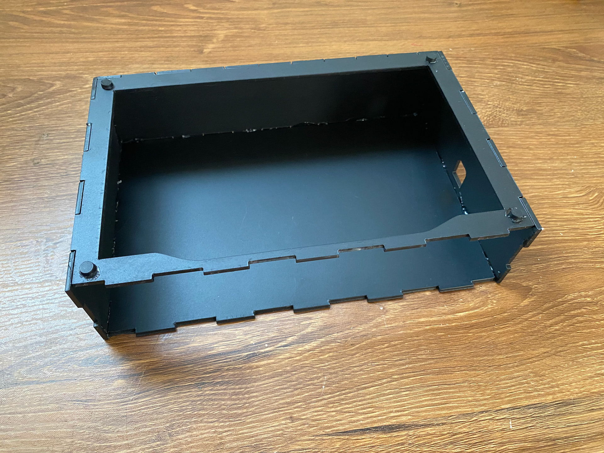
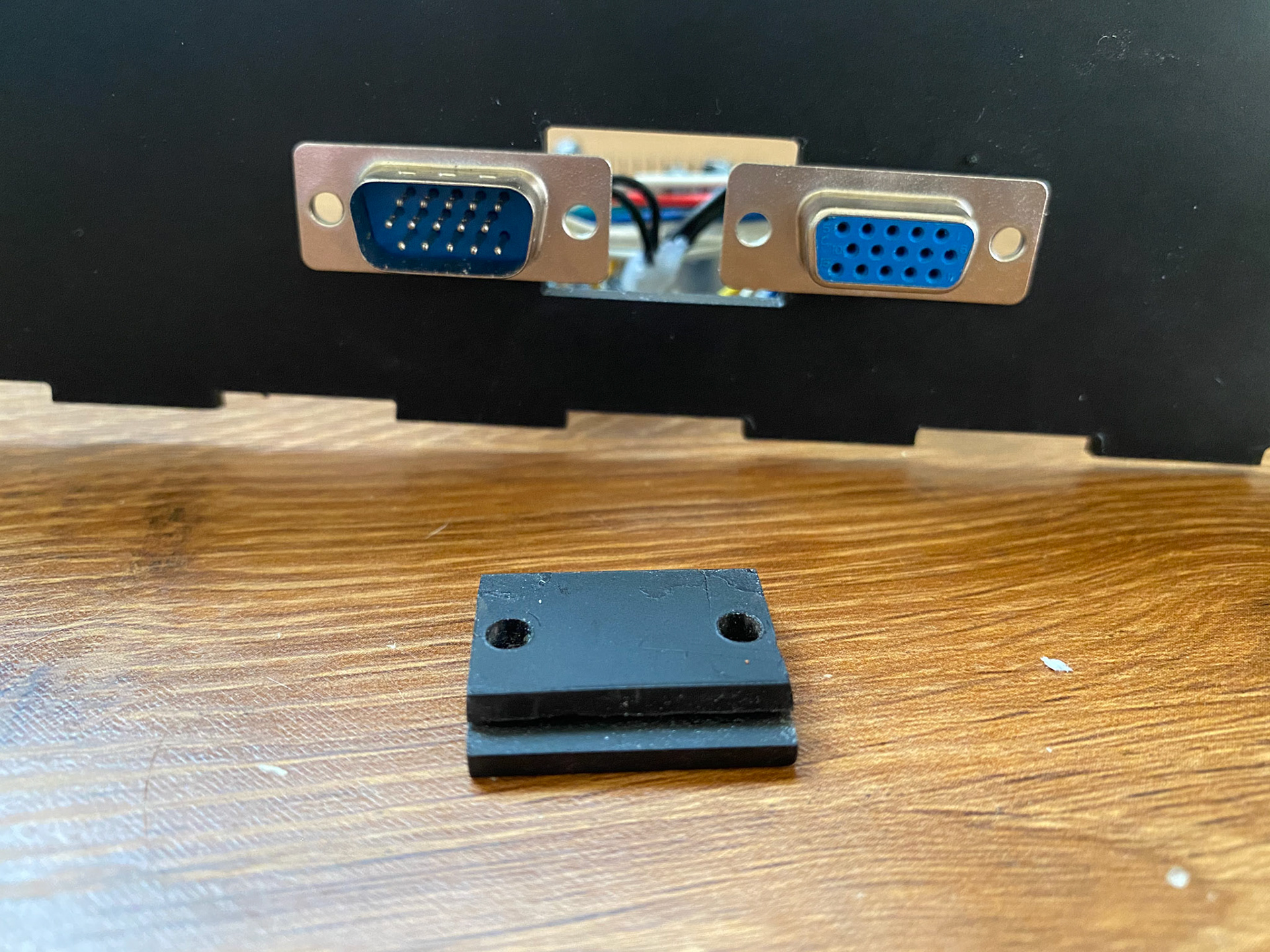
I actually had to cut 2 enclosures because I realized after attaching the first one together that I could not get the VGA inputs in front of the board where they needed to be without removing them from the board ad reattaching inside. To make sure that the VGA inputs could be mounted to the front with the electronics inside, I designed a large middle cutout between the two spaces for the VGA connectors and designed a 2-layer piece to fit in the middle hole once the connectors were attached. I painted and glued these two layers together, and once the VGA components were fit in, I glued the middle piece between them. I glued the side with the VGA connectors to the enclosure last with the PCB attached.